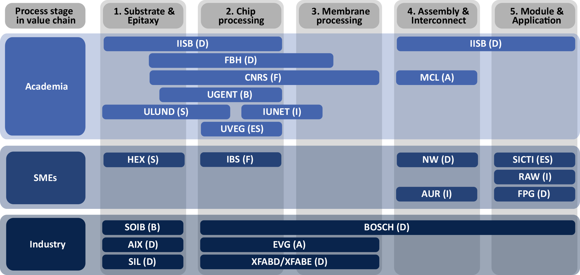
The consortium
The YESvGaN consortium consists of 23 European players located in seven countries from academia over SMEs to large industrial companies. The group is well balanced in order to contribute in a complementary way by key material, equipment, skills and knowledge needed for the ambitiously broad research and manufacturing field targeted by YESvGaN.
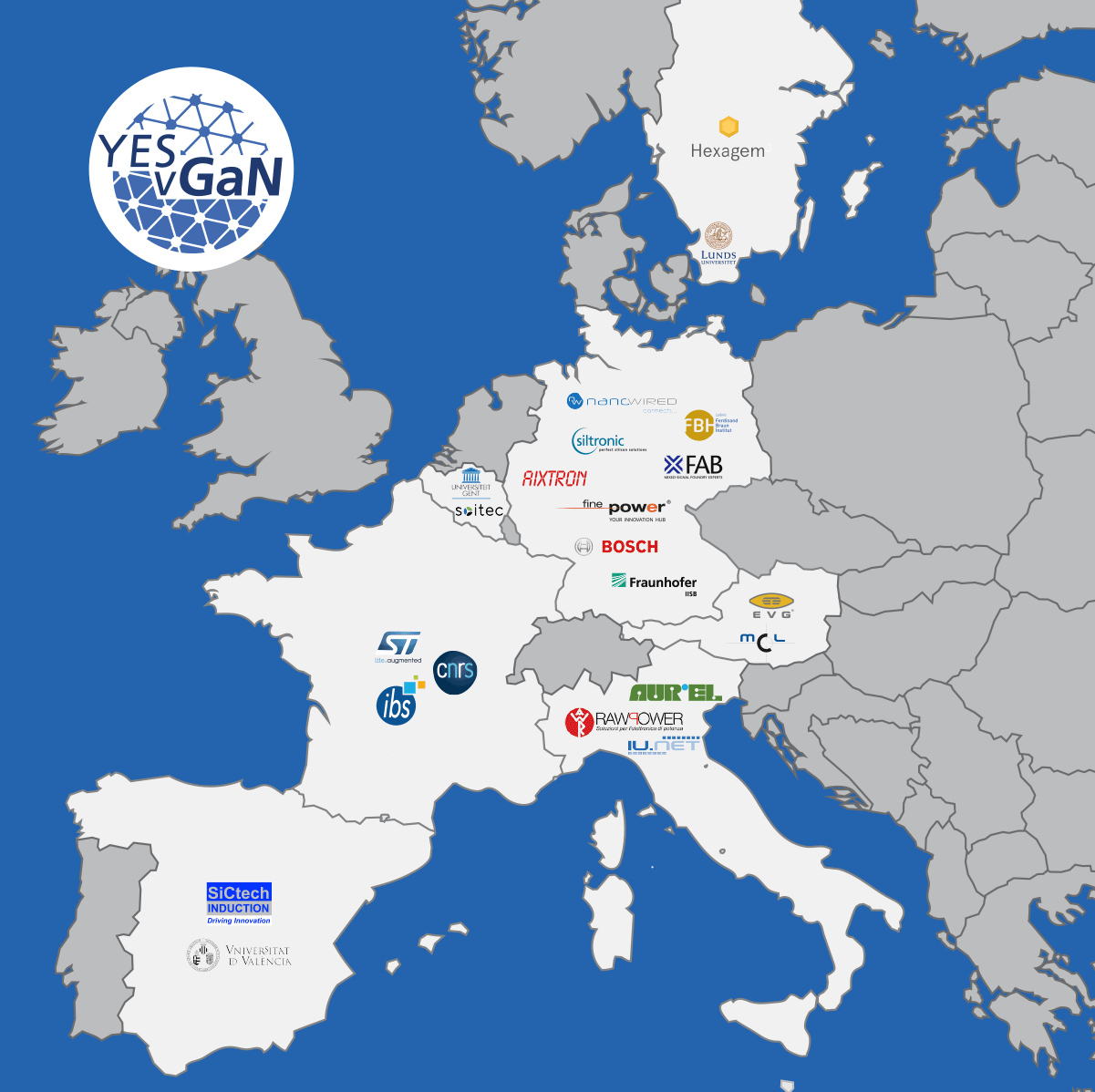
It is essential that the whole value chain from raw wafer to finished power module is present both from the manufacturing as well as from the metrology point of view. Partners from academia, SMEs and industry are spread along this value chain adding their perspective to the project at each stage, while several academic and industrial partners are active in more than one of the process stages. This will facilitate clarifying requirements from the start and foster collaboration between the work packages.
Overview of consortium as a whole
sorted by area of expertise and academia/SME/industry
 The Bosch Group is a leading global supplier of technology and services. It employs roughly 395,000 associates worldwide (as of December 31, 2020). The company generated sales of 71.5 billion euros in 2020. Its operations are divided into four business sectors: Mobility Solutions, Industrial Technology, Consumer Goods, and Energy and Building Technology. Bosch improves quality of life worldwide with products and services that are innovative and spark enthusiasm. In short, Bosch creates technology that is “Invented for life.” With its more than 400 locations worldwide, the Bosch Group has been carbon neutral since the first quarter of 2020. Mobility Solutions is the biggest Bosch Group business sector, accounting for 59 percent of total sales. Bosch is one of the leading automotive suppliers. In this role, it is pursuing a vision of mobility that is sustainable, safe, and exciting.
Besides its role as YESvGaN project coordinator, the Robert Bosch GmbH contributes to the project objectives as task leader and partner in chip technology and process development as well as in the advancement of joining and interconnection technology. Bosch will contribute with its expertise in power transistors and manufacturing of wide-bandgap power devices.
 AIXTRON SE is a leading provider of deposition equipment to the semiconductor industry. AIXTRON's technology solutions are used by a diverse range of customers worldwide to build advanced components for electronic and opto-electronic applications based on compound or organic semiconductor materials. Such components are used in a broad range of innovative applications, technologies and industries: Laser and LED applications, display technologies, data transmission, SiC and GaN power management and conversion, communication, signaling and lighting as well as a range of other leading-edge technologies.
AIXTRON is leading the WP2 activities which tackle current challenges related to epitaxy of GaN-based power devices. AIXTRON is playing a pivotal part in improving the epitaxial growth for large-area GaN growth on foreign substrates for vertical power devices and providing such material for the project partners. To further boost the market penetration of GaN-based devices, AIXTRON is exploring the field of epitaxial growth on 300 mm including the design, development and installation of a tool capable of depositing GaN layers on 300 mm Si substrates.
 Aurel is a well-established company founded in 1970 in Modigliana, Italy. Aurel’s Microelectronic division designs and manufactures custom microelectronic and automation solutions in particular for high power applications such as Thick Film on Ceramic type substrates, Power Module Assembly, Thick Wire Bonding & Glob Top, Silver Sintering, Hermetic Module Assembly, PCBA, Thick Film Heaters, Sensor Assembly, Led Assembly. The automation division designs and manufactures machines and automations for the electronic production mainly for applications in sensors, energy management and electronic modules.
Major tasks of Aurel in the project are improvements of the new vertical GaN devices by manufacturing solutions, testing of the semiconductors and different mounting solutions on ceramic and aluminum nitride substrates as well as test and validation of innovations regarding the top layer interconnection.
 CNRS – IEMN (Institute of Electronics, Microelectronics and Nanotechnology) is a Joint Research Unit created in January 1992 by the National Centre for Scientific Research (CNRS) and the University of Lille. Nearly 500 people of which a hundred international researchers work together at IEMN. The heart of our activities is centered on the micro and nanotechnologies and their applications in the fields of information, the communication, transport and health. Our researchers have at their disposal of the exceptional experimental means, in particular of the power stations of technology and characterization whose possibilities and performances are at the best European level.
CNRS-IEMN will contribute to several Work-packages such as WP2 (electrical evaluation of materials), WP3 (support to the frontside processing) and WP4 (Development of the backside local substrate removal and subsequent drain ohmic contacts, which is a key feature of these novel devices).
 EV Group (EVG) is a leading supplier of high-volume production equipment and process solutions for the manufacture of semiconductors, MEMS, compound semiconductors, power devices and nanotechnology devices. A recognized market and technology leader in wafer-level bonding and lithography for advanced packaging and nanotechnology, EVG’s key products include wafer bonding, thin-wafer processing and lithography/nanoimprint lithography (NIL) equipment, photoresist coaters, as well as cleaning and inspection/metrology systems. EVG is focused on delivering superior process expertise to its global R&D and production customer and partner base – from the initial development through to the final integration at the customer’s site.
In the project, EVG will develop industrial and scalable processes and equipment for temporary bonding and debonding, a laser-lift off process for GaN on sapphire and nanoimprint lithography for fin structuring in vertical FinFets.
 The Ferdinand Braun Institute gGmbH, Leibniz Institute for Highest Frequency Technology (FBH) researches electronic and optical components, modules and systems based on compound semiconductors. The FBH is a center of competence for III-V compound semiconductors covering the full range of capabilities, from design through fabrication to device characterization.
In YESvGaN will contribute by the development of vertical GaN FinFETs on Si and on Sapphire substrates for Laser-lift-of technology in cooperation with the project partners. This comprises the complete device design from epitaxy processing up to the final devices intended for tests in system environment. Further, FBH will develop low inductance high-speed packaging techniques for vertical GaN FETs based on AlN substrates.
 The Fraunhofer-Gesellschaft is the leading organization for applied research in Europe with 72 institutes and research units at locations throughout Germany. It employs a staff of more than 26,600, who work with an annual research budget totaling more than 2.5 billion euros. The main objective of the Fraunhofer Institute for Integrated Systems and Device Technology (IISB) is to provide excellent research to its customers and to set technological benchmarks as one of the leading research institutions in the field of electronic systems. For this, about 220 employees plus numerous students occupy a total area of approximately 7000 m² workspace. With various high-class laboratories allowing research and development on a broad range spanning power electronics systems and modules, semiconductor technology, and materials development.
Within YESvGaN, IISB provides its unique expertise in the analysis of materials microstructure and the identification of device limiting materials defects by a clever combination of sophisticated analytical measures. With the help of the wide range of equipment, e.g. plasma cleaning, printer for paste material, full automatic die placer with high temperature and extended tool force capability, automatic wire and ribbon bonders (Al, Cu, Au), servo presses for sintering, as well as resistance welding machines for electric terminals, the experts in assembly and interconnection technology deal with new types of interconnection technologies and module designs. On system level, the IISB will contribute with its experience in power electronic system simulation, circuit design and customized test benches for static and dynamic semiconductor characterization, which are optimized for wide bandgap applications.
 Finepower GmbH (FPG) is a leading company focused on innovative solutions in the field of power electronics. Since 2001 FPG is acting as a successful and professional partner for its customers and suppliers. By employing newest technologies and innovative solutions FPG contributes substantially to the reduction of energy consumption and efficient power conversion. Supported by advanced laboratory equipment and modern HW/SW tools, Finepower’s engineering team develops power electronic systems, complex magnetic power components and performs thermal and electrical simulations. The engineering core competence is on bidirectional power conversion from the 1~ and 3~ public grid with long experiences in developing battery chargers, grid converters and high power, high efficient DC/DC converters and wireless charging systems.
The tasks of FPG in within YESvGaN focus on the specification of transistor parameters with a clear view from application side to achieve a practically useful design. They include electrical simulation, e.g. for evaluation of switching losses and efficiency on a digital twin of a power electronics circuit using physical models of the GaN semiconductor technologies. FPG will especially investigate the performance in hard-switching configuration that is demanded in a three-phase power factor correction topology.
 Hexagem AB (HEX) is a Swedish company, founded in 2015 with the specific purpose of commercializing a newly established, nanowire based, substrate technology for power electronics and RF applications. HEX provides unique nanowire-based substrate technology that enables complementary exploration of cost-efficient GaN-on-Si for power applications. For the project, HEX can contribute by a vast infrastructure such as epitaxy, semiconductor processing or metrology at the ProNano pilot production line and the Lund Nano Lab at Lund University.
In the project, HEX will use and adapt its novel nanowire-based substrate technology to explore if thickness limitations of the drift region in GaN-on-Si can be relaxed or removed by using nanowire based GaN as the epitaxial basis of the drift region, neutralizing its dependence on the Si substrate. In particular, the company will be responsible for developing nanowire based low defect GaN template layers and will provide GaN templates for qualification and growth of thick drift layers by project partners.
 Ion Beam Services (IBS) is a French SME company set up in 1987 and is recognized as the European specialist of ion implantation. IBS offers a wide range of equipment and services for semiconductor companies: ion implanters (IMC/ FLEXION Beam Line tools and PULSION Plasma Doping tool), maintenance, retrofit and refurbishment of ion implanters and foundry services for Si and SiC. IBS is involved in process development for advanced devices for logic and power devices on Si and SiC. Further, IBS has developed a Plasma Immersion Ion Implantation tool (named PULSION) and a specific beam line implanter for compound substrates (SiC, AsGa,..). IBS has a clean room with several ion implanters able to implant on up to 300 mm wafers and also a fabrication line with lithography, deposition, etching and annealing tools for small and medium volume fabrication of sensors and high voltages devices on Si and SiC.
In YESvGaN, IBS will develop a specific Ion Implantation tool for GaN with the capability to reach high energy and to implant at high temperature. Further, IBS will collaborate with BOSCH, LIU, FBH and IEM for Ion Implantation and annealing process and associated model development.
 The “Consorzio Nazionale Interuniversitario per la Nanoelettronica” (IUNET, Italian Universities Nano-Electronics Team), is a non-profit private Organization, aimed to lead and coordinate the effort of the major Italian University Teams in the field of Semiconductor Device Modeling and Characterization. Two groups are involved in the present proposal: University of Padova (IUNET-PD), University of Modena e Reggio Emilia (IUNET-MORE). IUNET-PD (University of Padova) has a long-standing expertise in (i) Characterization of GaN based transistors for RF and power applications. (ii) Analysis of trapping processes limiting the dynamic performance of devices, development of physical models of the charge-trapping processes; study of the interface traps by C-V, Dit and Vth transient measurements. (iii) Study of the lifetime-limiting mechanisms in GaN-based transistors and diodes; time-dependent dielectric breakdown, instability of the p-type and insulator layers, hot electron effects (studied by electroluminescence), failure analysis. IUNET-MORE (University of Modena and Reggio Emilia) is involved in two research activities: TCAD simulation for reliability assessment and electrification fields. 1) The group has a consolidated experience in the use of TCAD simulations as a tool to investigate trap-related parasitic phenomena and high-field effects and to validate different device degradation models in GaN field-effect transistors 2) Electrification sector, research activity very well connected to industries in the territory. This activity focuses on the design of electrical drives for high-speed motors and their control, via GaN-based inverters. The research in the group ranges from basic technology and feasibility studies to actual demonstrators of electrical machines, electric drives, power electronics converters and relative test set-up
 Materials Center Leoben Forschung Gmbh (MCL) is an internationally active research institution in the field of applied materials science with around 160 employees. The research focuses on the digitalization of materials behaviour along the entire supply chain, from material synthesis via materials processing and manufacturing to components in service until their deployment. In March 2012, the MCL research area „Materials for Microelectronics“ was established with the objective to develop and investigate new material solutions for the micro- and nano-electronics industry. Technological innovations in the field of sensor integration, new models for load- and lifecycle calculations, new experimental approaches for materials analysis and new co-design approaches in order to reduce product development time are the main targets.
MCL contributes to the project objectives as task leader in work package 5 and partner in the analysis of thermal transport and reliability testing. MCL will contribute with its expertise to provide inputs for thermal design and for describing material degradation of the YESvGaN system.
 The NanoWired GmbH (NW) developed the Nanowiring Process for coating various surfaces with metallic nanowires. These coating are used for assembly of an interconnection technology, the NanoWiring. Based on this NW established the KlettWelding, KlettSintering and KlettGlueing processes, offering a wide range of advantageous process parameters for the assembly of electronic systems. NW’s equipment and manufacturing includes 6 NanoWiring production machines and a cleanroom with equipment for lithography, plasma cleaning and other sample preparation steps. For assembly NW has an ISO 8 cleanroom containing two Sinter presses and a Fineplacer.
In the project, NW will investigate the NanoWiring Structure and optimize the process for the AIT of the chips. Further, work topics are the fabrication of the nanostructures on substrates and wafers, assembly of the chips and basic reliability tests.
 Raw Power Srl (RAW) was born in 2007 as spin-off of the university of Modena and Reggio Emilia, from a close group of people dealing with power electronics. Nowadays Raw Power is a SME engineering company with less than 10 employees and its core business is the design and consultancy in static electric energy conversion, electrical machines design and electric power drives for industry applications.Raw Power's mission is promoting the technology transfer from the research scope to the enterprises. Raw Power can support its customers during product design and manufacture offering innovative and up-to-date solutions with the existing body of knowledge.
Beside its role in the YESvGaN project, Raw Power will be involved in the application phase of the project which aims to define technical data of the new vertical GaN power transistor and compare its performance with the one of the traditional WBG technologies in order to demonstrate vertical GaN advantages. Raw Power will bring its know-how to improve WBG technologies in industry applications.
 SiCtech INDUCTION, since 2017, it is a passionate team, combining young members and senior engineers with more than 30 years’ experience in the field, that puts all its energy at the service of the development of innovative and disruptive induction heating products. Our worldwide teams have given themselves the mission to provide to the market a breakthrough and totally innovative inverter/converter technology by using the latest semiconductor technologies enabling induction heating power supplies with extremely high efficiencies even at very high frequencies, very low size and weight high robustness, advanced features at very competitive prices.
The role of SiCtech, together with other partners, is the definition of requirements, from the industrial point of view, of the vertical GaN power devices as well as the development of a dedicated test bench and selected industrial prototypes for testing and qualification of the vertical mosfets developed in the project.
 Siltronic AG (SIL), headquartered in Munich (Germany), is one of the global semiconductor material leaders and is recognized as a technology leader in the design and production of highly specialized silicon wafers. The company with a long tradition is internationally positioned and partners with many preeminent chip manufacturers and companies in the semiconductor industry. Main products are high performing polished and epitaxial silicon wafers up to 300mm diameter. Employing a workforce of almost 3,800 members of staff, Siltronic commands a global network of advanced, leading edge production plants in Europe, Asia and the USA.
Major tasks in the project are the development of structures and epitaxy processes for vertical GaN stacks and the provision of 300mm Si wafers for the GaN MOCVD upscaling.
 Soitec is an industry leader in designing and manufacturing innovative semiconductor materials. The company uses its unique technologies and semiconductor expertise to serve the electronics markets. Soitec has manufacturing facilities, R&D centers and offices in Europe, the U.S. and Asia.
Soitec Belgium nv (SOIB) was incorporated as EpiGaN nv in 2010 as fully independent, hi-tech start-up, spin-off from imec. In 2019, EpiGaN was acquired by Soitec sa, and is integrated as a stand-alone business unit (BU). The BU EpiGaN commercially provides GaN-on-Si and GaN-on-SiC solutions for efficient power electronics, RF and sensor electronic devices and systems.
In YESvGaN SOIB will develop epitaxial layer stacks and processes for fabrication of vertical transistors on Si substrates. This includes buffer technology that allows growing thick GaN drift layers, background doping level reduction and control thereof as well as investigation of techniques to reduce the threading dislocation density in GaN on Si.
 STMicroelectronics is an independent worldwide broad-range semiconductor supplier and it is ranked in the top ten semiconductor companies (except foundries) in the world with a turnover of 9.56 billion USD in 2019. ST has 11 main production sites, more than 46 000 employees in 35 countries with 80 sales offices. ST is found everywhere microelectronics make a positive contribution to people's lives. STMicroelectronics (Tours) SAS (ST-T) is dedicated to development and production of discrete components in power conversion, and in the integration of active and passive devices. Tours site also hosts a Packaging R&D activity, including KGD (Known Good Die) process development for SiC products, and interconnection and package development for GaN products. On March 5th, 2020, STMicroelectronics has signed an agreement to acquire a majority stake in French Gallium Nitride (GaN) innovator Exagan.
In the project, ST-T will be responsible for the target specification of a vertical power diode, the assembly in a power package and electrical and reliability assessments.
 Ghent University is one of Belgium’s leading institutions of higher education and research. Established in 1817, it now hosts 47,000 students and 15,00 staff members. Ghent University is ranked 66th in the Shanghai and 103rd in the Times ranking. The research group CoCooN (Conformal Coating of Nanostructures) is part of the Department of Solid State Sciences at Ghent University. The group consists of 2 professors, 7 postdoctoral researchers and 10 PhD students, and is involved in thin film materials research, with a focus on Atomic Layer Deposition and thin film characterization. More information about the research group can be found at www.cocoon.ugent.be.
Being able to participate in the YESvGaN project enables Ghent University to build upon its existing infrastructure and expertise in the field of in situ thin film characterization and thin film deposition processes. In this way we aim to bring key novel insights to the field of power electronics.
 The Semiconductor Device Materials unit at University of Lund (ULUND) has activities on III-N and materials since 20 years. The focus has been on III-Ns for high-frequencies and light-emitting applications and on terahertz and infrared ellipsometry techniques for electronic properties characterization. Besides growth (both bulk and epitaxy) performance-limiting defects have been a major research topics. ULUND hosts a world-leading comprehensive materials research facility, with wide resources in growth and characterization equipment, and expertise.
Tasks of ULUND in the project are contactless THz and IR ellipsometry characterization of the electrical properties of epitaxial materials and the device structures, growth of thick GaN layers on GaN nanowire templates on Si, comparative characterization of the structural and electrical properties of device structures on nanowire templates and on super lattice templates, and implantation and activation of n-type and p-type doping species (e.g. Si, Mg).
 The University of Valencia (UVEG) was founded in 1499. It is one of the oldest, largest, and most important universities in Spain covering 92 departments and 16 research institutes. UVEG is within the top five universities in the global Spanish rank (teaching-research-innovation) for research. Our research group is integrated in the Institute of Materials Science (ICMUV), created with the aim of coordinating research interests in the field of advanced materials and nanomaterials. Our team specializes in the optical and electrical characterization of nanostructures with sub-micrometre resolution and pico-ampere currents applied to the characterization of III-nitride materials, nanowire-based devices, and new hybrid systems with carbon-based materials.
UVEG contributes to YESvGaN as expert in the optical micro and nanoscale characterization of nitride semiconductors, temperature mapping of wide-bandgap power devices by means of Raman thermometry and the modelling of their thermo-mechanical properties
 X-FAB is the leading analog/mixed-signal and MEMS foundry group manufacturing silicon wafers for automotive, industrial, consumer, medical and other applications. Its customers worldwide benefit from the highest quality standards, manufacturing excellence and innovative solutions by using X-FAB’s modular CMOS and SOI processes in geometries ranging from 1.0 µm to 130 nm, and its special silicon carbide and MEMS long-lifetime processes. X-FAB’s analog-digital integrated circuits (mixed-signal ICs), sensors and micro-electro-mechanical systems (MEMS) are manufactured at six production facilities in Germany, France, Malaysia and the U.S which have a combined capacity of approx. 100,000 eight inch equivalent wafer starts per month. X-FAB employs about 3,800 people worldwide. As partners on the chip technology and membrane processing work packages, X-FAB Dresden and X-FAB Erfurt contribute its process development expertise on a commercial 200 mm CMOS line to manufacture the Vertical GaN power transistor. This includes the front-side source and gate module processing at X-FAB Dresden as well as the backside processing with special care for the local substrate removal, backside drain formation and metallization at the X-FAB Erfurt location. This is expected to lower the adoption barrier of wide bandgap materials for power conversion applications.
You can find us on

